



Yalantis provides full-cycle FPGA design services for medical, industrial, automotive, and connected IoT hardware, taking programmable logic from architecture and RTL through verification to board bring-up and production. Our FPGA engineers work alongside the firmware and cloud developers who build the rest of your product, in an ISO-certified R&D lab in Warsaw.
FPGA Design Services for Mission-Critical Hardware


ISO
13485
Medical devices
IEC
62443
Industrial security
ISO
27001
Information security
ISO
9001
Quality management
ISO
27701
Privacy management
Years in engineering
18+
Expert Engineers
50+
Hardware projects delivered
30+
In-house lab in Warsaw
R&D
Full-cycle FPGA design and development services
One integrated team takes your programmable-logic project through every phase, from the first architecture decision to production-ready bitstreams.
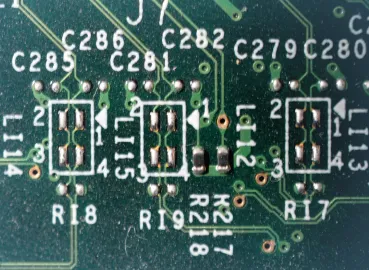
Architecture and specification
We define the FPGA architecture before any RTL gets written, since these are the decisions that are expensive to unwind later. Our aim is a design your engineers can review and push back on while changes are still cheap.
- Device and family selection weighed against resource needs and long-term availability
- Resource budgeting across logic, memory, DSP, and transceiver blocks
- Clock domain plan and reset strategy settled up front
- Interface definitions and register maps agreed with the firmware side
- Hardware and software partitioning for SoC FPGA targets

RTL design in VHDL, Verilog, and SystemVerilog
Our engineers write synthesizable RTL that reads clearly and holds up as the design grows. Discipline here is what saves weeks later in verification and timing closure.
- Reusable, parameterized modules in the HDL your team already maintains
- Clean clock-domain crossings and proper reset synchronization
- Coding standards and automated linting applied to every module
- State machines and datapaths written for predictable synthesis results
- Code that ports across device families and vendor toolchains

Functional verification and timing closure
We build the verification environment in step with the design, so testing keeps pace with the RTL. When a block is called done, coverage data is what settles it.
- Self-checking testbenches in UVM or cocotb
- Constrained-random stimulus backed by directed tests for corner cases
- Functional and code coverage tracked against a written verification plan
- Static timing analysis and constraint refinement until the design closes
- Verification report covering the evidence and any remaining risk

Synthesis, place and route, and bitstream generation
We take the verified design through implementation and out the other side as a production bitstream. Because every build runs from scripts, the same result is still reproducible months later.
- Synthesis and implementation in Vivado, Quartus Prime, Libero, or Radiant
- Floorplanning and pin assignment for congested or timing-critical designs
- Timing and utilization reports reviewed at each iteration
- Version-controlled build flows any engineer on the project can rerun
- Bitstream generation with encryption and secure boot where required

Board bring-up and integration
Our team follows the design onto real hardware and runs bring-up in our Warsaw lab. This is where assumptions in the schematic meet a scope probe, so we plan for it well before the boards arrive.
- Schematic and pin-planning review before boards go to fabrication
- First power-up and configuration checks on prototype hardware
- Debug with JTAG, integrated logic analyzers, and bench instruments
- Signal integrity measurements on high-speed nets
- Joint debug with the firmware team on register and driver behavior

IP integration and high-speed interfaces
We integrate vendor IP and build custom logic for the fast interfaces your product depends on. From there, the links get proven on real silicon against the protocol specification.
- Vendor and third-party IP cores configured and validated in-system
- Custom blocks where off-the-shelf IP does not fit the requirement
- PCIe, Ethernet, MIPI, USB, and DDR interface implementation
- Memory controller bring-up with calibration and margin testing
- SerDes tuning with eye diagram and bit error rate measurement
Explore industries we work with
SoC FPGA design services
Why ship a separate processor and FPGA when one chip can carry both? A SoC FPGA combines an Arm or RISC-V processor with programmable logic on a single device, so your software and your custom acceleration share the same silicon. The hard part is making the two halves work as one, and that is exactly what we design, all the way through to bring-up.



FPGA platforms and toolchains we work with
We are vendor-independent and select the device family that fits your performance and lifecycle needs. Our engineers are fluent across the major FPGA vendors and their toolchains.

AMD / Xilinx
AMD adaptive SoCs and high-end FPGAs for compute and networking, designed in Vivado and Vitis.

Intel / Altera
From low-cost Cyclone designs to high-performance Agilex and Stratix devices, built in Quartus Prime.

Microchip
Low-power, flash-based, and security-focused FPGAs from the former Microsemi portfolio, designed in Libero SoC.

Lattice
Small, low-power FPGAs for edge and embedded vision, designed in Radiant and Diamond.

VHDL

Verilog

SystemVerilog

Chisel

HLS

C/C++

Vivado

Vitis

Quartus Prime

Libero SoC

Radiant

Diamond

UVM

cocotb

Questa

VCS

Verilator
DO-254 (awareness)
Compliance & certifications

ISO 13485
Medical device quality management

IEC 61508
Functional safety standard
for industrial and electronic systems

ISO 27001:2022
Information security across systems and processes
ISO 11898
(CAN) communication standard
used in automotive and industrial systems

ISO/SAE 21434
Cybersecurity standard for road vehicles

UN R155 / R156
Regulations for vehicle cybersecurity and software updates
IEC 62304
Governs the lifecycle of software within medical devices
IEC 60601
Electrical safety and performance requirements
for medical devices

CE
Required to sell hardware in the EU

FCC
Required for devices with
electromagnetic emissions in the US

UL
Certification for electrical safety,
widely required in North America.

RoHS
Restricts hazardous
materials in electronics

IPC-A-610 / IPC CID
Standards for PCB design
and assembly quality
Why companies choose Yalantis as their FPGA design partner
Yalantis is a hardware and software engineering partner. The same company handles FPGA design, embedded firmware, and cloud development for your product, under one certified process.

In-house R&D lab with full hardware capability
Our R&D lab in Warsaw takes an FPGA design from RTL all the way through bench bring-up and validation, all in one place and all under ISO 9001. The same engineers who wrote the logic are the ones assembling and testing the prototype boards.
Compliance-first workflows for regulated products
We build the design records that map to whatever standards your product has to meet, whether that is IEC 62304 and IEC 60601 for a medical device or IEC 62443 for an industrial system. Compliance is part of how we work from the first day, so it never becomes a scramble at the end.
FPGA logic designed by the team that writes the firmware
Our FPGA engineers sit with the embedded and Rust developers who write the firmware around the chip, so they design register maps and driver interfaces with the software in mind. That is why integration tends to go faster, with fewer surprises at bring-up.
One partner from logic to cloud
Beyond the FPGA itself, the same company handles PCB design, firmware, embedded software, and the cloud backend. You deal with one engineering partner across the whole product, instead of stitching a chain of vendors together.
How our FPGA design process works
A structured, milestone-driven workflow with built-in review and compliance checkpoints, from discovery through production support.

Discovery and requirements engineering
We start by capturing the functional, timing, power, and regulatory requirements for the design. Target device class and certification goals are agreed before architecture work begins.

Architecture and specification
Next, we define the FPGA architecture and partition the design into clock domains and functional blocks. For SoC FPGAs, we also decide what runs in software and what belongs in programmable logic.

RTL design and IP integration
From there, engineers write synthesizable RTL and integrate vendor or third-party IP. Your team joins module-level reviews against coding standards and the agreed specification.

Functional verification and timing closure
We verify each block and the full design with self-checking testbenches and coverage metrics. Static timing analysis and constraint refinement bring the design to timing closure on the target device.

Synthesis, place and route, and bitstream
Once verification is on track, we run synthesis, place and route, and bitstream generation through scripted, reproducible build flows. Reports on timing and resource utilization are reviewed at each iteration.

Board bring-up and hardware integration
After that, we bring the design up on prototype hardware in our lab. The FPGA is validated together with the firmware and the surrounding board, with rapid iteration driven by real measurements.

Production handoff and sustaining support
Finally, we hand over the complete design package: source RTL, constraints, build scripts, bitstreams, and documentation. We support production ramp-up and later engineering changes as the product evolves.
How we work together
-
Time and Materials (primary)
Our primary model for FPGA work. You get a flexible team that scales with the project while requirements evolve, billed for the effort actually spent. Ideal for R&D and designs where the scope is still taking shape.
- R&D and evolving scope
-
Dedicated team
A long-term team of FPGA, firmware, and hardware engineers embedded in your roadmap, led by a dedicated project lead. Ideal for multi-device product lines and ongoing development programs.
- Ongoing product development
-
Discovery and fixed-price scoping
Once FPGA is the agreed direction, a short fixed-price engagement turns your concept into a costed project plan with a delivery estimate and a milestone breakdown. A low-commitment way to plan the build before committing to a full program.
- Planning a chosen build
-
AI-enabled team
A team set up with enterprise-grade AI tooling so delivery moves faster. We work only on licensed corporate AI platforms with strict data isolation, so your IP stays protected. It runs as an AI-accelerated pod with built-in pipelines for automated code review and test generation, and the documentation stays current as the design evolves.
- Speed to market
Two ways to get started
Not sure FPGA is the right path?
Get a fixed-price architecture assessment and a clear recommendation in 2 to 3 weeks.
FPGA design your auditor can read
We deliver the logic and the full traceability package for your 510(k) or IEC 62443 review.
Testimonials from our clients





FPGA design services insights
Articles
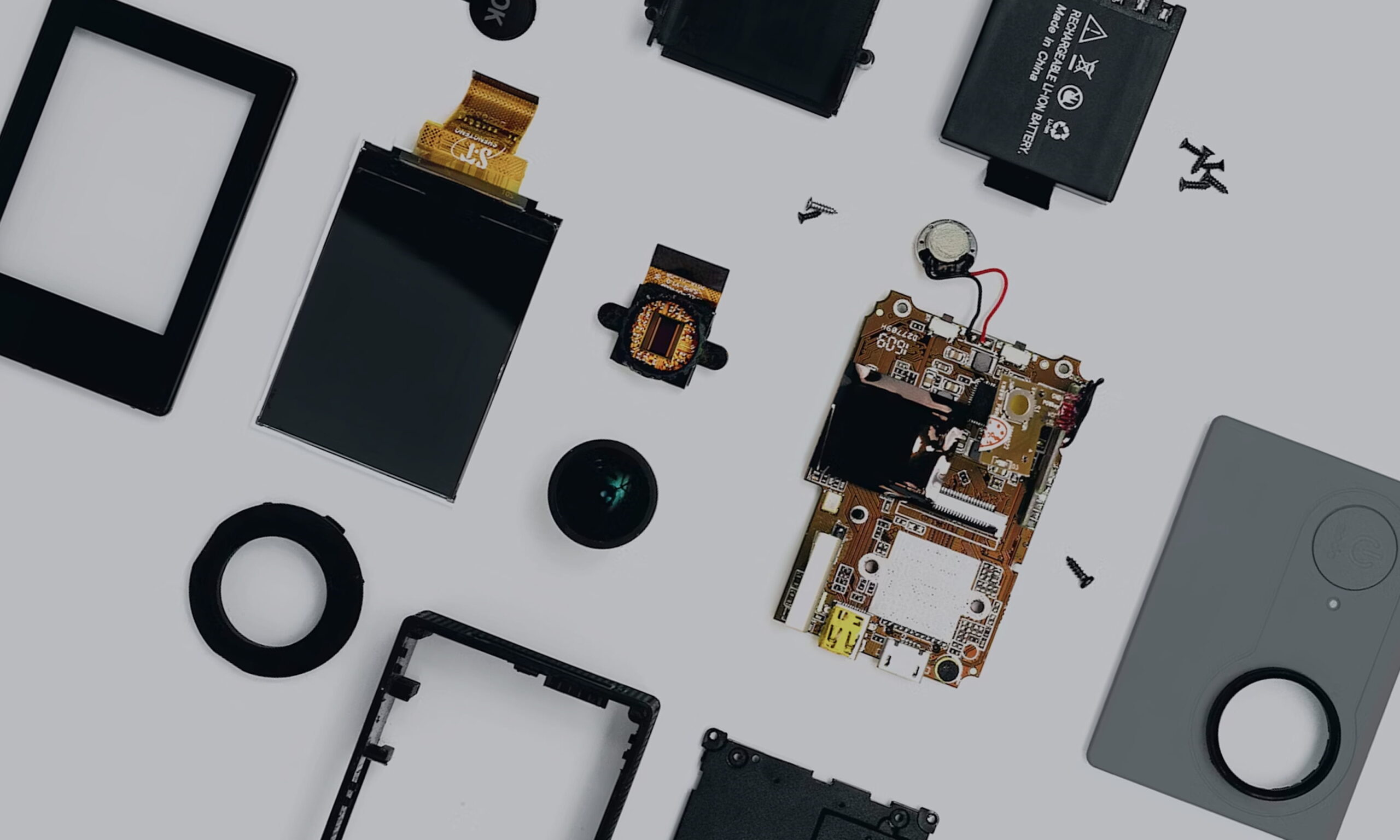
How to Reduce BOM Costs Without Sacrificing Product Quality
Discover how to reduce BOM costs without sacrificing product quality. Learn how early design decisions and hardware architecture improvements lower manufacturing costs at scale.

Articles
What Are the Key Steps to Designing Medical Sensors?
Designing medical sensors for IoT? Don’t miss this breakdown of hardware, firmware, connectivity, and privacy essentials.

Articles
How to Build a Wearable App in 2026: A Full-Stack Guide from Hardware to Cloud
Find out how healthcare facilities can improve quality of services, boost patient engagement, and reduce costs for hospital visits by adopting wearable tech. Build your own wearable app with Yalantis wearable technology developers.

Articles
How to Integrate Medical Wearable Technologies With EHR Systems in Hospitals and Clinics
Learn why you absolutely have to add wearable health devices into your healthcare facility EHR, and how it will benefit your patients and healthcare providers.
Articles
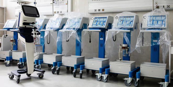
Ways in which remote patient monitoring devices assist in fostering patient trust and positive business image
Explore how the adoption of remote patient monitoring devices can open up lots of opportunities for healthcare businesses, generate new revenue streams, and foster patient trust.
Talk to our FPGA design engineers
Whether you need a verification effort on an existing design or a full-cycle FPGA development program, our hardware engineering team is ready to scope your project.
Related services
FAQ
-
Which FPGA platforms and vendors do you support?
We design across the major FPGA vendors: AMD/Xilinx (Versal, UltraScale+, 7-Series, Zynq), Intel/Altera (Agilex, Stratix, Arria, Cyclone), Microchip (PolarFire, PolarFire SoC, SmartFusion), and Lattice (Nexus, CrossLink, CertusPro, ECP5). We work in Vivado, Vitis, Quartus Prime, Libero SoC, Radiant, and Diamond, and we select the device family based on your performance and lifecycle requirements rather than a single vendor relationship.
-
What is SoC FPGA design and when is it the right choice?
A SoC FPGA places an Arm or RISC-V processor system on the same chip as programmable logic, so application software and custom hardware acceleration run side by side. It is the right choice when a design needs both general-purpose computing and deterministic, low-latency hardware, for example running an operating system such as Linux while processing a sensor stream in real time, a pattern common in embedded systems. Devices such as AMD/Xilinx Zynq, Intel/Altera Agilex SoC, and Microchip PolarFire SoC are common targets. Our SoC FPGA design services handle the hardware and software partitioning and the bring-up of both domains.
-
How does Yalantis ensure FPGA design quality for regulated industries?
Quality is built into the process through coding standards, linting, and coverage-driven verification, backed by milestone reviews with your engineers. For regulated products we maintain traceable design records that map to the relevant standards, including IEC 62304 and IEC 60601 for medical devices, IEC 62443 for industrial systems, and ISO 26262 awareness for automotive electronics. Yalantis holds ISO 9001, ISO 13485, ISO 27001, and ISO 27701 certifications, and our verification evidence is structured to support your certification submissions.
-
How long does an FPGA design project take?
Timelines depend on complexity and device class. A contained block or a verification effort can run a few weeks, while a full SoC FPGA design with high-speed interfaces and regulatory documentation typically takes several months from kickoff to a production-ready bitstream. Our milestone-driven process keeps the schedule transparent. Share your requirements and we will provide a tailored estimate.
-
Do you offer FPGA verification as a standalone service?
Yes. We take on functional verification and timing closure as a standalone engagement, whether the RTL was written in-house or by another vendor. We build self-checking testbenches and coverage models in UVM or cocotb, then reproduce and isolate any failures on the design. You receive a verification report documenting the evidence and the remaining risks. This is a common entry point for teams that need extra capacity or an independent check before tape-in.
-
Can FPGA design be combined with PCB and firmware development?
Yes, and this is where Yalantis is strongest. The same R&D company delivers PCB design, firmware, embedded software, and cloud development alongside FPGA work. Running these together means the FPGA and the board it sits on are designed together with the software that drives them, which reduces integration risk and shortens bring-up.
How to get started with Yalantis
Leave your info and a few words about the project. We’ll review it and reach out to book a call.
Welcome to Yalantis, please fill out the form and we’ll get back to you.

Thank you for contacting us.
Keep an eye on your inbox. We’ll be in touch shortly
Meanwhile, you can explore our hottest case studies and read
client feedback on Clutch.