
|
Key takeaways
|
Bringing a physical product to market is exciting work, and unforgiving in a way software rarely is. Break code and you patch it by Friday. Get a board or a mold wrong and the fix gets expensive fast, while your earliest choices set the cost and timeline of the program.
So this guide is about getting those early calls right. It walks the full lifecycle, the stack from enclosure to cloud, the compliance that gates your launch, and the question most teams face first: build in-house, or partner?
What is hardware development, and why is it harder than software?
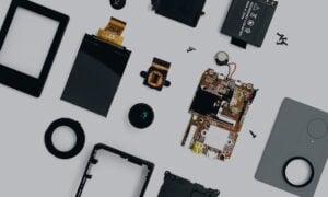
Hardware development is the end-to-end process of designing, engineering, prototyping, testing, and manufacturing a physical electronic product you can produce reliably and at scale, within the regulations of its market. Hardware design and development is harder than software for one reason above all: change is slow and expensive, and once a product ships you often cannot fix a physical defect remotely at all.
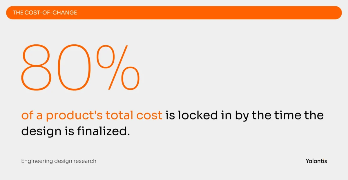
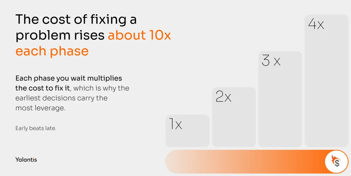
That single fact is why your earliest decisions carry the most weight. Research on engineering change shows the cost of fixing a problem grows by roughly a factor of ten with each successive lifecycle phase, and that up to 80% of a product’s total cost is locked in by the time the design is finalized. A rib you add to an enclosure during concept work costs almost nothing; the same change after the mold is cut can run into tens of thousands and slip your start of production. Early beats late.
The term stretches further than most people expect. It covers the mechanical enclosure, the printed circuit board, the firmware that brings the silicon to life, and the cloud services the device talks to. A smart insulin pump or an industrial edge gateway: each is the output of hardware development, and each is a system rather than a gadget.
That systems framing shapes how Yalantis approaches hardware product development. Yalantis is a full-cycle hardware and software development company that builds connected products from PCB to cloud, with compliance engineered in from the first requirement rather than added at the end, an approach we call Compliance-First Engineering. Most modern devices fail in the gaps between disciplines, so owning the full scope is what keeps those gaps from opening.
Hardware development vs. hardware design vs. hardware engineering: what’s the difference?
These three terms describe different scopes, and confusing them leads to scoping mistakes in contracts and team structure, so it is worth being precise.
Hardware design is the creative and technical specification work: deciding what the product should do and how its parts should fit and connect. Schematic capture and component selection live here, along with enclosure industrial design. Hardware engineering then makes that design real and reliable, owning signal integrity, thermal behavior, power budgets, EMC, and manufacturability.
Hardware development is the umbrella over both. It includes design and engineering, and it adds prototyping, verification, compliance, manufacturing readiness, and the sustaining work that follows launch. So when someone asks what a hardware developer actually does, the honest answer is that the role sits across all of it, coordinating specialists rather than owning a single board.
How is hardware development different from software development?
The core difference is the cost and speed of change, and almost everything else follows from it. In software you iterate in minutes and patch after release; in hardware a single board revision can take weeks and real money, and a shipped defect may not be fixable in the field at all.
That single fact reshapes planning, budgeting, team structure, and risk tolerance. The table below lays out the differences that most often trip up teams arriving from a pure software background.
| Dimension | Software development | Hardware development |
|
Iteration speed |
Minutes to hours |
Days to weeks per board respin; months for tooling |
|
Cost of a late change |
Low, often a redeploy |
High, up to 10x more per lifecycle phase |
|
Fixing defects after launch |
Over-the-air patch |
Recall, field service, or non-recoverable |
|
Regulatory exposure |
Usually low |
High: FCC, CE, ISO, IEC certifications gate the launch |
|
Supply-chain dependency |
Negligible |
Critical: component lead times and single-source risk |
|
Cost locked in early |
Moderate |
Up to 80% fixed at design freeze |
|
💡 Pro tip |
The hardware development life cycle: the 7 phases where cost and risk concentrate
The hardware development life cycle is the structured sequence of phases that takes a product from idea to volume manufacturing and beyond. Most teams use a 5 to 8 phase model; we use seven, because it maps cleanly to where cost and risk actually pile up.
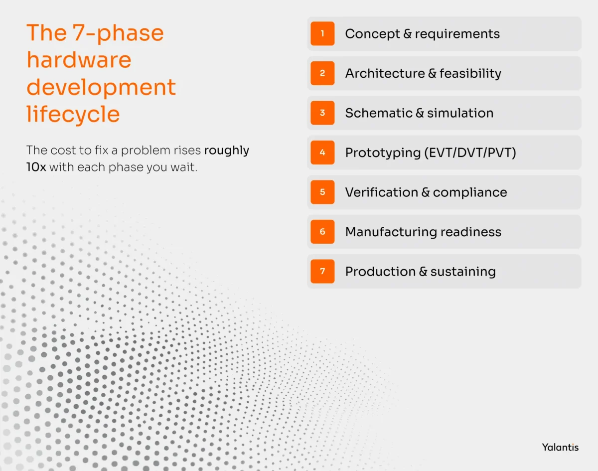
Every competitor guide organizes itself around phases, so treat this as table stakes done properly. The reason to name the hardware development process explicitly is that each phase carries its own deliverables and typical duration, plus its own way of going wrong, and once you can see those failure modes coming you can plan against them. What follows walks each phase of the hardware product development process through its objective and the mistake that most often derails it, with the deliverables and durations gathered in one table at the end.
Phase 1: Concept and requirements definition
This is where you decide what the product must do and for whom, translating customer needs into the constraints it has to meet, and it produces the single document every later decision traces back to. Get the product requirements specific and the whole program has solid ground to build on.
Leave them vague and you pay for it later. If technical requirements like rugged or low power never become numbers, your engineers will fill the gap with guesses, and those guesses resurface as expensive surprises around phase six. This is also the moment to pin down your target markets, because the regulatory requirements they impose can reshape the architecture before you have drawn a single schematic.
Phase 2: System architecture and feasibility
With requirements set, you decide the high-level structure: what runs on a microcontroller versus an FPGA, which connectivity standard fits, where the compute lives, and what is achievable inside your cost and power budgets. The output is an architecture you can commit to and a clear view of what still needs proving.
The mistake here is skipping feasibility on the one subsystem that scares you. That unproven RF link or aggressive thermal target is exactly what should be de-risked first, while change is still cheap and a redesign costs days instead of months.
Phase 3: Schematic design and simulation
Now the design process turns the architecture into detailed electronic design, and you validate it virtually before committing to physical boards. Schematic capture and selection of electronic components happen here, checked against SPICE and signal-integrity simulation, so the board you eventually fabricate behaves the way the model promised.
The trap is choosing components for their specs alone. A flawless design built around a chip on a 52-week allocation is not a design you can ship, so lead time and lifecycle status belong in the selection criteria from the start.
Phase 4: Prototyping (alpha, beta, EVT/DVT/PVT)
Prototyping turns the design into physical hardware in escalating stages, and each build is iterative by design because each one answers a different question. Hardware prototype development moves from rough proof to production-ready confidence in steps.
Alpha and beta builds test functionality and design intent. The formal sequence then tightens the screws. EVT (engineering validation) confirms the design works. DVT (design validation) confirms it meets every requirement, and PVT (production validation) confirms the factory can build the final product at quality and volume. Rushing past EVT to hit a demo date is how unvalidated assumptions slip into DVT, where they cost ten times more to unwind.
Phase 5: Verification, validation, and compliance testing
This phase proves, through electrical and functional testing, that the product meets its requirements and that you can comply with the regulations of every market you intend to sell in. It is also where too many programs discover, far too late, that compliance is a long-lead activity rather than a final checkbox.
Certification labs book out weeks ahead, and a failed EMC scan can force a board respin that resets your schedule. The fix is structural: build compliance checkpoints into every earlier phase so nothing arrives here as a surprise. That habit is the heart of Compliance-First Engineering, and it is the difference between a smooth gate and a frantic one.
Phase 6: Manufacturing readiness (DFM, DFA, pilot run)
Manufacturing readiness makes a validated design economical and repeatable to build. Design for manufacturing (DFM) and design for assembly (DFA) strip out cost and defect risk before you commit to volume, and a pilot run proves the line can hold quality at scale.
The recurring error is engaging your contract manufacturer late. Bring DFM input in during schematic design instead, because engineering-change research shows a modification made after tooling costs far more than the same change during early design, often by an order of magnitude or more.
Phase 7: Production, sustaining engineering, and end-of-life
The final phase covers the production processes for volume manufacturing and the long tail that follows: managing component obsolescence, pushing field updates, monitoring quality, and eventually retiring the product responsibly. This is where launch reveals itself as a milestone along the way, with real work still ahead of you.
Suppliers and manufacturers change their catalogs, components go obsolete, security threats evolve, and a fleet in the field needs a way to receive firmware updates safely. Regulations like the EU Cyber Resilience Act now require security support across a product’s entire supported lifetime, so a sustaining plan is no longer optional housekeeping.
| Phase | Primary objective | Key deliverables | Typical duration | Common failure mode |
|
1. Concept & requirements |
Define what to build and for whom |
PRD, cost/BOM budget, target certs, risk assessment |
2 to 6 weeks |
Vague, unquantified requirements |
|
2. Architecture & feasibility |
Decide system structure, de-risk the hard parts |
Block diagram, make/buy, security architecture |
3 to 8 weeks |
Skipping feasibility on the risky subsystem |
|
3. Schematic & simulation |
Detail and validate the electronics virtually |
Schematics, SPICE/SI sims, sourced BOM |
4 to 10 weeks |
Components with bad lead time or near end-of-life |
|
4. Prototyping (EVT/DVT/PVT) |
Build and prove the design physically |
Alpha/beta boards, EVT/DVT/PVT results |
2 to 4 months |
Rushing past validation gates |
|
5. Verification & compliance |
Prove requirements and regulatory readiness |
Test reports, EMC/safety results, cert docs |
Weeks to many months |
Compliance treated as a final gate |
|
6. Manufacturing readiness |
Make it cheap and repeatable to build |
DFM/DFA review, pilot run, second sources |
4 to 12 weeks + tooling |
Engaging the manufacturer too late |
|
7. Production & sustaining |
Scale, maintain, and retire responsibly |
Ramp support, OTA pipeline, EOL plan |
Full product life |
Treating launch as the finish line |
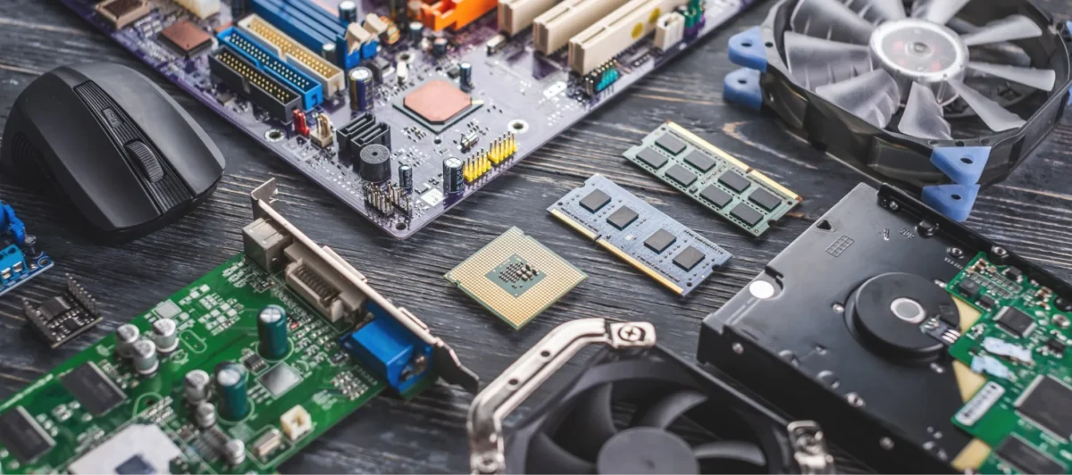
The hardware development stack: why the seams between PCB and cloud break first
A connected product is a stack of layers that has to behave as one system, and the integration risk almost never lives inside a layer. It lives in the seams between them. The full-cycle view, running from mechanical enclosure through PCB, firmware, connectivity, and cloud, is what separates a device that ships from a pile of subsystems that almost integrate.
Most competitor guides stop at the board, which is exactly why their readers get blindsided later. The walkthrough below takes each layer in turn and shows where it hands off to the next, linking to the dedicated deep dive wherever you need more depth than a pillar should carry.
Mechanical and enclosure design
Mechanical and enclosure design defines the physical body of the product: its form, fit, thermal management, and ingress protection. It decides whether the device survives its environment and feels right in a user’s hand, and it constrains the electronics from the outside in, since enclosure volume and heat dissipation both push back on the board.
PCB design and layout
PCB design and layout turns the schematic into the physical board that carries every component and signal. The layout choices made here, on routing and grounding especially, decide its signal integrity and EMC performance. This is one of the most failure-prone layers precisely because a clean schematic can still produce a board that fails an EMC scan.
FPGA and digital logic
FPGAs and programmable digital logic handle the high-throughput or low-latency processing a general microcontroller cannot, which makes them a natural fit for signal processing, including DSP, and custom interfaces. They also help your schedule, because reconfigurable logic is one of the cheaper layers to iterate, so it absorbs late changes that would be ruinous in silicon.
Electronic product design
Electronic product design is the connective layer that ties the electronics and mechanics to the user experience in one coherent product. At this level, electronic hardware development keeps performance and cost honest about the usability they have to support, so the device works as a whole rather than as a set of parts that each work alone.
Firmware and embedded software
Firmware and embedded software are the code that runs directly on the device, controlling the hardware and exposing its behavior, and this is where embedded hardware development meets the software world. It is also where timelines quietly slip, because firmware for embedded IoT devices gets treated as a finishing touch when it belongs on the critical path.
The modern shift here is toward memory-safe languages for safety-critical code, which we come back to in the next section.
Building firmware that has to stay reliable and secure in the field?
Our firmware engineers write embedded code in Rust and C, with safe over-the-air updates built in.
Connectivity, cloud, and device management
This top layer covers how the device connects and talks to the cloud, and how you manage a whole fleet of units in the field, from the protocol choice down to the over-the-air update path that keeps devices current and secure. It is the layer pure electronics shops tend to drop, and it is exactly where regulators now focus their attention.
|
💡 Pro tip Put one architect in charge of the seams between layers, on top of your per-layer owners. In full-cycle programs the expensive surprises almost always surface where firmware meets PCB, or where the cloud’s update model collides with the device’s memory budget. |
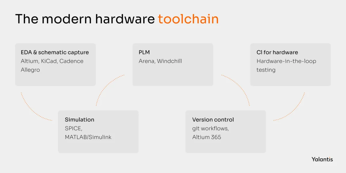
Which tools and technologies actually speed up hardware development
Modern hardware development tools span electronic design, simulation, lifecycle management, and a set of newer software practices that make devices safer. The right toolchain pays for itself by shortening iteration loops and helping you optimize the design before it reaches a physical board, where fixing problems gets expensive.
Here is the practical landscape your team will work in day to day:
- EDA and schematic capture: Altium, KiCad, and Cadence Allegro, the PCB design software for schematic design and board layout.
- Simulation: SPICE for circuit analysis and MATLAB/Simulink for system and signal modeling, so behavior is validated before fabrication.
- PLM: Arena and Windchill to manage BOMs, revisions, and change orders across the lifecycle.
- Version control for hardware: git-based workflows and platforms like Altium 365 that bring software-style change tracking to electronic design.
- CI for hardware: hardware-in-the-loop (HIL) testing that automates validation against real or simulated devices.
Two emerging technologies deserve a closer look from any leader planning a multi-year roadmap, because both change what is possible at the edge.
The first is Rust for safety-critical firmware. Memory-safety bugs are the dominant security problem in low-level code: CISA and the NSA report that roughly 70% of serious security vulnerabilities stem from memory-safety issues, and both agencies now urge a shift to memory-safe languages. Rust closes off entire classes of those defects at compile time, which is why it is gaining ground fast in automotive and medical firmware. Yalantis was an early commercial adopter, and what we learned from putting Rust to work in IoT firmware is that a mixed Rust-and-C codebase captures most of the safety gain without forcing a full rewrite.
The second is TinyML for on-device intelligence. Running compact machine-learning models directly on the device cuts latency and cloud cost while keeping sensitive data local, which matters as much for privacy as it does for performance.
Want memory-safety designed into your firmware from the start?
Our Rust engineers build safety-critical embedded code that rules out whole classes of bugs at compile time.
Why agile hardware development only works as a hybrid
The reason is the cost-of-change curve. Pure software-style Scrum, the staple of agile software development, assumes you can fail fast and rewrite freely, and that assumption breaks the moment a change means a new board spin or a recut mold instead of a code push. So the honest starting point is to name where Scrum stops working before describing the model that does. Getting this line wrong is one of the most expensive mistakes in the field.
You cannot fail fast and iterate on a $40,000 injection mold the way you iterate on a web feature. An agile methodology for hardware development has to bend its agile principles around where iteration is cheap and where it is ruinous, and the model that holds up in practice draws a line between the two: stage-gate discipline for the expensive, irreversible commitments, and fast agile sprints inside the phases where change is nearly free.
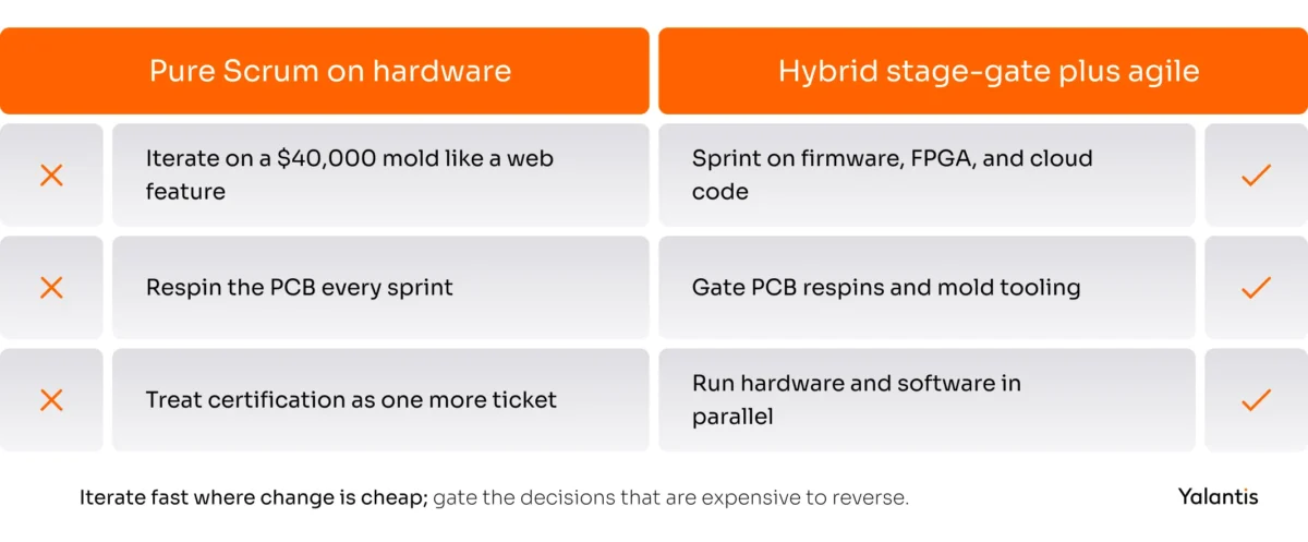
Where iteration is cheap, run it hard:
- Firmware and embedded software, which you can rebuild and reflash in minutes.
- FPGA and reconfigurable logic, which you can re-synthesize without new silicon.
- Cloud, connectivity, and device-management code.
Where iteration is expensive, slow down and gate the decision:
- PCB respins, which cost weeks of fabrication and assembly per cycle.
- Mechanical tooling and molds, where rework runs into tens of thousands.
- Certification, where a single failed test can reset a multi-week lab queue.
The cadence that ties this together runs hardware and software in parallel instead of in sequence. Firmware sprints proceed against stable interfaces and prototype boards while the next board revision sits in fabrication, so neither side waits on the other. The discipline that makes parallel work possible is keeping the contract between the two stable enough that firmware never has to chase a moving target.
|
💡 Pro tip Define your hardware-software interface (pinouts, registers, protocols) as a versioned contract, and freeze it before firmware sprints begin. The single most productive thing you can do for parallel work is stop the interface from shifting underneath your firmware team. |
Running hardware and embedded software in parallel?
Our embedded software team builds the on-device code that ships in lockstep with your hardware.
Compliance decides whether you can ship, so build it into every phase
Compliance is the strongest single determinant of whether you can legally sell a hardware product, and treating it as a phase-five gate is the surest way to wreck a timeline. The way out is to map every certification to the phase where its evidence actually has to be generated, so the work is spread across the program instead of crammed at the end.
This is the territory most guides skip, and it is where Yalantis concentrates. We hold ISO 13485 for medical devices, plus ISO 27001 and ISO 27701 for security and privacy, and we wire compliance milestones into each phase rather than chasing them at the finish.
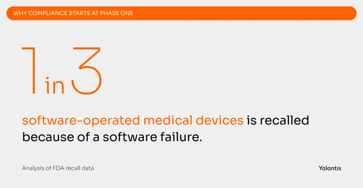
The stakes are easy to underestimate until you see them in numbers. In medical devices, analysis of FDA recall data shows roughly one in three software-operated devices is recalled because of a software failure, and a recall is the most expensive way imaginable to learn that validation belonged earlier.
ISO 13485 for medical devices

ISO 13485 is the quality management standard for medical device design and manufacturing, and in regulated markets it decides whether you can sell at all. It demands traceability from requirement to test, which means your documentation discipline has to start at phase one rather than catch up at the end. For connected products it pairs with software standards like IEC 62304, and a program like the behind-the-ear hearing aid Yalantis delivered through the FDA 510(k) pathway lives or dies on exactly that early planning.
IEC 62443 for industrial control systems

IEC 62443 is the security standard for industrial automation and control systems, and it grows more mandatory as factories connect operational technology to IT networks. Because it addresses the OT-IT integration risk that comes with brownfield modernization, it shapes decisions back in phase two; retrofitting segmentation and secure communication into a finished design is painful and slow.
ISO 26262 for automotive functional safety

ISO 26262 governs functional safety for road-vehicle electronics, defining how you prevent and contain failures in systems where a fault can endanger life. Its ASIL risk levels drive the rigor of your design, and the evidence accumulates across the entire lifecycle rather than in a final audit. It is also one of the clearest reasons automotive firmware is moving toward memory-safe languages.
ISO 27001 and ISO 27701 for data security and privacy

ISO 27001 covers information security management and ISO 27701 extends it to privacy, and together they define how you protect data and prove that protection to enterprise buyers. They matter most at the connectivity and cloud layer, where the device’s data leaves the building, and procurement teams at large customers increasingly require both before they will sign.
FCC, CE, the EU Cyber Resilience Act, and market-specific requirements

FCC marks in the US certify electromagnetic compatibility and radio compliance, while CE marks in the EU also cover electrical safety, and without the right mark the device cannot legally go on sale. The newest and most consequential addition to this list is the EU Cyber Resilience Act. It entered into force in December 2024, with reporting obligations from September 2026 and full obligations from December 2027, and it mandates secure-by-design engineering and a software bill of materials, plus security updates across a product’s supported lifetime. With non-compliance fines reaching 15 million euros or 2.5% of global turnover, the time to plan lifecycle security support is now, well ahead of 2027.

Why IoT compounds every hardware development challenge
IoT hardware development takes every challenge in this guide and stacks them, because the device has to be cheap, low-power, connected, and secure all at once. The scale explains the stakes: IoT Analytics counts about 18.5 billion connected IoT devices, heading toward 39 billion by 2030, and each one carries the full weight of the constraints below.
Those constraints are unforgiving at the edge. The device fights for every milliwatt of power and kilobyte of memory, down to the last cent of BOM cost, and it still has to stay reliably connected and genuinely secure. Connectivity, then, is an architecture decision rather than a late add-on:
- Cellular (LTE-M, NB-IoT, 5G): wide-area coverage for mobile or remote assets, at higher power and module cost.
- LoRaWAN: long range and very low power for low-data sensors.
- Wi-Fi: high bandwidth where mains power and local networks exist.
- BLE: short-range, low-power links to a gateway or phone.
Security has the same early-or-painful character, designed in from the silicon up with secure boot and encrypted communication, plus a trustworthy over-the-air update path. The EU Cyber Resilience Act has effectively turned secure-by-design into a legal requirement for connected products sold in Europe, so the architecture you choose now is the one regulators will hold you to later.
Building a connected product that has to reach the cloud?
We take IoT devices from PCB to cloud, with connectivity and device management handled as one stack.
Where hardware development demands the most: four industries
Some industries push the engineering bar far above the baseline, because failure here can cost lives or trigger serious liability. Matching your market to its specific demands is the fastest way to see where your effort and budget should concentrate.
Healthcare and medical devices
Healthcare hardware carries the heaviest regulatory burden of any vertical. ISO 13485 and IEC 62304 set the quality standards and software bar, while the FDA or EU MDR pathway gates every connected medical device, from IoMT hardware to software-as-a-medical-device. The schedule killer here is usually certification delay rather than engineering difficulty, and the talent gap is real, because you need hardware and embedded engineers working alongside regulatory expertise in one team.

Industrial manufacturing
Industrial hardware lives or dies on OT-IT integration and IEC 62443 compliance, set against the reality of brownfield modernization, where new gateways have to talk to equipment that predates them by decades. PLC integration and edge gateways are common entry points, and reliability targets are punishing, since downtime on a production line is counted in lost revenue per minute. Our AI predictive maintenance system work sits squarely in this space.
Automotive
Automotive hardware development centers on ECU development and the move toward software-defined vehicles, with over-the-air updates part of that same shift, all under the rigor of ISO 26262 functional safety. The bar for safety-critical electronics is among the highest anywhere, which is a leading reason the industry is adopting memory-safe firmware: a single defect can carry safety consequences. It is also where named clients like Toyota Tsusho operate.
Logistics
Logistics hardware prioritizes asset tracking and cold-chain monitoring, plus ruggedization for devices that spend their working life in motion and weather. Battery life and connectivity in low-coverage areas are the recurring engineering constraints, and the volume economics reward aggressive BOM optimization, where shaving a few cents per unit across a large fleet quickly adds up to real money.
Build in-house or partner? A framework for choosing a hardware development company
The build-versus-partner decision comes down to five factors: internal capability, time-to-market pressure, regulatory burden, the capital cost of lab equipment, and your appetite for risk. There is no universal answer, but the pattern becomes clear the moment you score yourself honestly against all five.
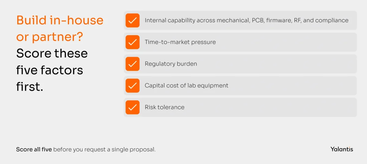
Two of those factors are easy to underestimate. Custom hardware development demands a rare mix of specialists across mechanical, PCB, firmware, RF, compliance, and manufacturing, and few companies keep that full development team on staff. The capital side bites just as hard, because EMC chambers and environmental test rigs, plus a prototyping lab, cost serious money before you build a single sellable unit. Use the matrix below to find where you sit:
| Factor | Lean toward building in-house | Lean toward a hardware development partner |
|
Internal capability |
You already employ the full discipline mix |
You have gaps in PCB, firmware, RF, or compliance |
|
Time-to-market |
Long runway, no hard launch date |
Pressure to hit a market window quickly |
|
Regulatory burden |
Low, or you hold the certifications |
High, with ISO/IEC pathways you have not run before |
|
Capital for lab equipment |
Already invested, or hardware is core long-term |
You want to avoid heavy fixed-cost investment |
|
Risk tolerance |
High, and hardware is a strategic core competency |
Lower, and you want shared delivery risk |
Read the matrix and the conclusion tends to write itself. If hardware will be a long-term core competency and you can absorb the ramp-up cost, building internal capability pays off over time. If you face a regulated market or real capability gaps under a tight deadline, a hardware development partner takes the slowest risks off your critical path.
This is where full-cycle delivery earns its keep. Yalantis runs an in-house R&D lab in Warsaw covering industrial design, PCB, prototyping, and firmware under one roof, with cloud and compliance attached, so the hardware-to-cloud handoffs that usually cause coordination pain simply happen inside one team.
Leaning toward a partner for the capabilities you can’t staff?
Our hardware development service covers mechanical, PCB, firmware, and cloud under one roof, with compliance engineered in from day one
|
💡 Pro tip Score the five factors above before you request a single proposal. Teams that skip this step tend to outsource the parts they already understand and keep the parts they should have handed off, which is almost always compliance. |
The most common (and most expensive) hardware development mistakes
Most hardware programs fail in predictable ways, and nearly all of those failures share one root cause: deferring an expensive decision until the phase where it is most expensive to fix. Here are the ones we see most, and what to do instead.
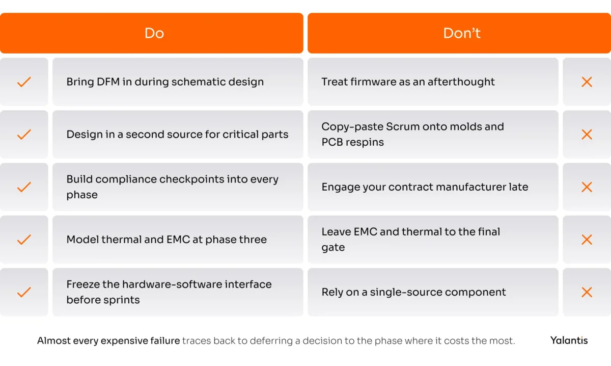
- Underestimating compliance lead times. Certification labs book out weeks ahead, and a failed scan can force a respin, which makes compliance the single most common schedule killer when it is left to the end.
- Treating firmware as an afterthought. Firmware belongs on the critical path, so starting it late, once the hardware is finished, quietly adds months you did not budget for.
No DFM until late. Bring manufacturing input in only after design freeze and you invite costly redesigns, because so much of the unit cost is already locked in by then. - Single-source component risk. One sole-source part on long allocation can halt an entire production line, so design in a second source from the start.
- No early thermal or EMC strategy. Thermal and EMC problems discovered at compliance testing are the ones that trigger board respins, which is why they belong in your phase-three models.
- Copy-pasting agile from software. Applying pure Scrum to mold tooling and PCB respins ignores the cost-of-change curve; the hybrid model exists precisely to avoid that trap.
Build your hardware product with a full-cycle partner
Yalantis delivers hardware development end to end, with hardware, firmware, cloud, and compliance under one roof. Our in-house R&D lab in Warsaw covers industrial design, PCB, prototyping, and firmware, and we are certified to ISO 13485 for medical devices, plus ISO 27001 and ISO 27701 for security and privacy. Clients including Toyota Tsusho, Bosch, and KPMG trust us with programs where compliance and reliability are not optional.
FAQ
What are the phases of hardware development?
Hardware development typically runs through concept and requirements, system architecture and feasibility, schematic design and simulation, prototyping (EVT/DVT/PVT), verification and compliance testing, manufacturing readiness, and production with sustaining engineering. Most teams use a 5 to 8 phase model, and the seven-phase version maps cleanly to where cost and risk concentrate.
What is the difference between hardware design and hardware development?
Hardware design is the specification work of deciding what the product does and how its parts fit and connect. Hardware development is the broader process that includes design, plus engineering, prototyping, compliance, manufacturing, and post-launch support. In short, design is a phase inside development.
How long does hardware product development take?
A connected consumer or industrial device usually has a development cycle of 12 to 24 months from concept to volume production. Regulated products such as medical devices take longer, because certification pathways add months of validation and documentation work that cannot be compressed.
Does agile work for hardware development?
Yes, as a hybrid with stage-gate rather than as pure Scrum. Run agile methods where iteration is cheap, such as firmware and cloud code, and use staged gates for expensive, irreversible commitments like PCB respins and mold tooling.
What are the main types of hardware?
Hardware spans consumer devices, industrial and embedded systems, medical and automotive electronics, and IoT or connected devices. Each type of hardware device development carries different constraints on cost, power, reliability, and regulatory exposure, which is why the same lifecycle gets weighted differently across industries.
What does a hardware developer do?
A hardware developer coordinates the design, engineering, prototyping, testing, and manufacturing of a physical electronic product. The role sits across mechanical, electronic, firmware, and compliance disciplines, usually orchestrating specialists rather than owning a single layer.
When should you outsource hardware development?
Outsource when you have capability gaps in PCB, firmware, RF, or compliance, or when a regulated market and a tight launch window make in-house capability too slow or costly to build. Build in-house when hardware is a long-term core competency and you can absorb the ramp-up.
How do you ensure compliance during hardware development?
Map every required certification to the phase where its evidence must be generated, and build compliance checkpoints into each phase instead of testing only at the end. This Compliance-First Engineering approach is what prevents the late-stage failures that force board respins and recalls.
About the author