
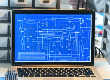
End-to-end printed circuit board design services for medical devices and industrial controllers, automotive electronics and connected IoT hardware. From schematic capture to manufacturing handoff, designed by the team that writes the firmware and builds the cloud.
PCB Design Services for Mission-Critical Hardware

ISO
13485
Medical devices
IEC
62443
Industrial security
ISO
27001
Information security
ISO
9001
Quality management
ISO
26262
Automotive safety
Years in engineering
17+
Engineers on staff
400+
Hardware projects delivered
200+
In-house lab in Warsaw
R&D
Why companies choose Yalantis for PCB design
Yalantis is a professional PCB design and hardware engineering partner. The same team handles PCB design and layout, embedded firmware, and cloud platform development for your product.
In-house R&D lab with full hardware capability
Our Warsaw R&D lab handles everything from schematic capture and PCB layout to prototype assembly and validation testing. All under one roof, all under ISO 9001.
Certified workflows for medical and industrial compliance
Design history files for FDA 510(k) submissions, IEC 62443 security-by-design for industrial controllers, ISO 26262 functional-safety-aware layouts for automotive ECUs. Compliance is integrated into the process from day one.
Firmware-aware layout, designed by the team that writes the code
Our PCB designers work alongside embedded firmware and cloud engineers. Pin assignments and debug interfaces are designed with the software architecture in mind from day one. Peripheral routing reflects real firmware requirements.
Production handoff with vetted EMS partners
We generate manufacturing-ready Gerbers, ODB++, assembly drawings, and pick-and-place files. We coordinate directly with vetted EMS partners so your board transitions from design to volume production without re-spin.
Our full-cycle services
Our PCB design capabilities cover every phase of circuit board design, from initial schematic capture through signal integrity verification and production-ready output. All handled by a single integrated team.

Schematic design and capture
Architecture definition, component selection, schematic capture in Altium Designer, Cadence Allegro, OrCAD, PADS Professional, or KiCad. Design reviews against regulatory requirements for your target industry.
Custom PCB layout services
Component placement optimization and controlled impedance routing for high-frequency and high-speed differential pairs. Multilayer, HDI, flex, and rigid-flex layout design. Mixed-signal partitioning ensures clean separation between analog and digital domains. ECAD-MCAD integration ensures the board fits the mechanical enclosure and thermal solution from the layout stage.

Signal and power integrity analysis
Pre-layout and post-layout SI/PI simulation using Ansys and HyperLynx. Eye diagram analysis and power distribution network impedance profiling identify issues early. Crosstalk mitigation strategies are validated with Keysight ADS.

Design for manufacturing (DFM) and testability (DFT)
Automated DFM checks verify design rules against IPC-2221 and your EMS partner’s capabilities. Test point placement and boundary scan design ensure ICT/FCT fixture compatibility.
Component selection and BOM optimization
Active lifecycle monitoring and multi-source strategies for supply chain resilience. BOM management ensures you hit your target price point. We flag obsolescence risks before they become production stops.

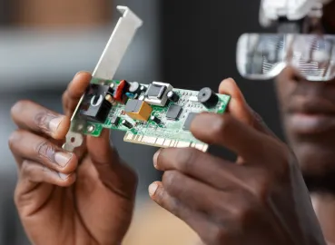
Prototyping and production handoff
Prototype coordination with vetted fab houses and bring-up testing in our Warsaw lab. Design iteration is driven by real test data. Complete manufacturing package delivery includes Gerbers and ODB++.
Explore more


Talk to our PCB design experts
Whether you need a second opinion on an existing board or a full-cycle PCB development program, our hardware engineering team is ready to scope your project.
How our PCB design process works
A structured, milestone-driven workflow with built-in compliance checkpoints, from discovery through volume production.

Discovery and requirements engineering
We begin by defining the electrical, mechanical, environmental, and regulatory requirements. Stack-up design, thermal budget, EMC strategy, and target certifications are documented before a single trace is routed.

Schematic design and component selection
Next, we define the architecture and verify active component lifecycles, paired with a multi-source BOM strategy. Your engineering team joins us for schematic reviews against IPC standards and industry-specific compliance requirements.

PCB layout and routing
From there, we move into footprint design and floorplanning followed by placement optimization and routing in Altium Designer or Cadence Allegro. Controlled impedance, length-matched differential pairs, and mixed-signal isolation are all reviewed against DFM rules specific to your EMS partner.

Verification: SI/PI, thermal, EMC pre-compliance
Once the layout is complete, we run post-layout signal integrity and power integrity simulations. Thermal analysis and EMC pre-compliance review identify issues before the first prototype, reducing re-spin risk and accelerating time to certification.

Prototype, test, iterate
After that, we coordinate prototype fabrication through vetted partners. Boards are assembled and tested in our Warsaw lab, with rapid design iteration driven by results while firmware integration testing runs in parallel.

Manufacturing handoff and production support
Finally, we deliver the complete manufacturing data package: Gerbers, ODB++, IPC-2581, BOM, assembly drawings, pick-and-place files, and 3D STEP models. We coordinate with your EMS partner and support through first-article inspection and pilot production.
Start with a scoped engagement
Two structured entry points designed for teams with specific design needs, a clear scope, and fixed timeline with defined deliverables.
PCB design review: pre-production risk assessment
Have an existing schematic or layout designed in-house or by another vendor? We review it for signal integrity issues, DFM violations, component obsolescence risks, and regulatory compliance gaps. The output is a structured report with prioritized fixes.
Deliverables:
- Signal integrity and power integrity assessment
- DFM/DFT rule check against your target EMS
- Component lifecycle and obsolescence risk audit
- Compliance gap analysis for target certifications
- Prioritized remediation report with cost estimates
Custom carrier board design for Raspberry Pi CM / Arm SoM
Productizing on a Raspberry Pi Compute Module or Arm-based System-on-Module? We design a custom carrier board tailored to your product requirements, covering interfaces, form factor, power, and certification readiness.
Deliverables:
- Custom schematic based on your SoM and I/O requirements
- PCB layout optimized for your enclosure and thermal constraints
- Production-ready BOM with multi-source components
- Gerbers, assembly drawings, and EMS handoff package
- Firmware bring-up support and integration testing
What you receive
Manufacturing package
- Manufacturing-ready Gerbers, ODB++, and IPC-2581
- Bill of Materials with approved vendor list
- Assembly drawings and pick-and-place files
- 3D STEP models for mechanical integration
- Fabrication notes and stackup specification
Verification and compliance
- SI/PI analysis reports and eye diagrams
- Thermal simulation results
- EMC pre-compliance documentation
- Design history files for regulated industries
- Test specifications and validation plans
How we work together
-
Dedicated PCB design team
A full-time team of PCB designers and firmware engineers with a dedicated project lead, embedded in your product development workflow. Ideal for multi-board product lines or ongoing R&D programs.
→ Ongoing product development
-
Project-based engagement
A fixed-scope, milestone-driven project with defined deliverables and timeline. From single-board design to complete hardware development programs with firmware and cloud integration.
→ New product launch
-
PCB design consultation and review
Expert assessment of your existing PCB design, covering schematic review, layout audit, DFM check, and compliance gap analysis. A low-commitment entry point that delivers actionable improvements.
→ Pre-production validation
Tools and standards we work with

Altium Designer

Cadence Allegro

OrCAD

PADS Professional

KiCad

Ansys

HyperLynx

Keysight ADS

COMSOL Multiphysics
IPC-2221 IPC-A-610 IPC-6012

ISO 13485 ISO 26262
IEC 60601 IEC 62304
Testimonials from our clients


Why choose Yalantis as your IoT integration company
Compliance-first approach
We hold ISO 13485 (medical devices), ISO 27001 (information security), ISO 27701 (privacy management), and IEC 62443 (industrial cybersecurity) certifications. These certifications shape how we architect, develop, and deploy every IoT integrated solution. For enterprises in regulated industries, this means your integration partner already speaks the language of your compliance team.
In-house R&D lab in Warsaw
Our Warsaw-based hardware lab handles PCB design, prototyping, firmware development, and cloud integration under one roof. When your project requires custom edge gateways or sensor boards, we design and test them in-house rather than outsourcing to a third party. This shortens feedback loops, improves scalability, and gives you a single point of accountability for the entire stack, from hardware to cloud.
Trusted by enterprise leaders
We work with organizations like Toyota Tsusho, Bosch, KPMG, and RAKwireless on projects that require both technical depth and operational reliability. These partnerships run for years, not months, because our IoT integration solutions are built to grow alongside their business needs.
Full-cycle capability
From hardware design and firmware development through edge computing, cloud architecture, and enterprise system integration, we cover the full stack. You do not need to coordinate between a hardware vendor, a firmware shop, and a cloud integrator. One team, one backlog, one delivery pipeline. Single team accountable from architecture through deployment and ongoing support.
Your IoT systems need proper integration architecture
Connect legacy equipment to enterprise systems without protocol conflicts or security gaps.
PCB design insights

Articles
The Ultimate Guide to IoT Testing: Catch Failures Before Your Customers Do
Master the complexities of IoT quality assurance with our comprehensive guide. Learn how to validate device-to-cloud synchronization and ensure ironclad security across your entire IoT network.
Articles
Embedded Medical Device Software: IEC 62304 & ISO 13485 Explained
If you’re preparing to scale an embedded medical device, this guide breaks down how IEC 62304 and ISO 13485 fit into your workflow and what you need to stay compliant as you grow.

Articles
How to Prevent Firmware Vulnerabilities with Secure Boot and OTA Updates
Discover how to prevent firmware vulnerabilities and how to keep connected devices secure, compliant, and recoverable at scale.

Articles
How to Integrate Medical Wearable Technologies With EHR Systems in Hospitals and Clinics
Learn why you absolutely have to add wearable health devices into your healthcare facility EHR, and how it will benefit your patients and healthcare providers.

Articles
Why Digital Display Labeling is Essential for Pharmaceutical & Life Sciences Industry
Digital Display Labeling: Eliminating paper label risks and enhancing supply chain agility in pharmaceutical clinical trials.
Related services
Hardware development
Firmware development
Embedded software development
IoT зroduct вevelopment
Medical sevices development
Mechanical design services
Electronic product design
FPGA Design
FAQ
-
What is included in your PCB design services?
Our custom PCB design services cover the full development lifecycle: requirements engineering, schematic design and capture, component selection and BOM optimization, multilayer PCB layout and routing, signal and power integrity analysis, DFM/DFT verification, prototype coordination, and complete manufacturing handoff packages including Gerbers, ODB++, assembly drawings, and 3D STEP models. For regulated industries, we also deliver design history files and compliance documentation alongside certification support materials.
-
What certifications and standards do you follow for PCB design?
Yalantis maintains ISO 13485 (medical devices) and ISO/IEC 27001 (information security) certifications alongside ISO 9001 (quality management). Our PCB design workflows are built to support FDA 510(k) submissions (21 CFR 820), IEC 60601 and IEC 62304 for medical devices, IEC 62443 for industrial cybersecurity, and ISO 26262 for automotive functional safety. All designs follow international quality standards including IPC-2221 and IPC-A-610, as well as IPC-6012.
-
Can you handle full PCB design and manufacturing, or just design?
Yalantis is a PCB design and engineering company focused exclusively on the design phase. We manage the complete journey from schematic to production by coordinating with vetted EMS partners for PCB manufacturing and assembly. We generate production-ready manufacturing packages and support your board through first-article inspection, pilot runs, and volume production ramp-up.
-
How long does a typical PCB design project take?
The timeline depends on complexity. A custom carrier board for a well-defined SoM can be designed in 6 to 8 weeks. A complex multilayer board with high-speed interfaces and mixed-signal design under regulatory compliance requirements typically takes 12 to 18 weeks from kickoff to production-ready output. Our structured process with milestone reviews keeps timelines predictable and transparent. Reach out to our team with your project details and we will provide a tailored estimate.
-
Do you provide PCB design consultation and design reviews?
Yes. Our PCB Design Review is a structured pre-production risk assessment where we audit an existing schematic or layout, whether designed in-house or by an external vendor. We evaluate signal integrity, power integrity, DFM compliance, and component lifecycle risks alongside regulatory readiness. The output is a prioritized remediation report. This is our most popular entry point for new clients.
-
Do you work with legacy PCB designs that need updating?
Absolutely. We regularly take over legacy PCB designs for re-engineering, whether the goal is component substitutions due to obsolescence, performance improvements, or cost reduction. We can work from existing Gerbers and schematics, or even from a physical board through reverse engineering, to deliver an updated, manufacturing-ready design.
-
Do you provide hardware design as part of IoT integration?
Absolutely. We regularly take over legacy PCB designs for re-engineering, whether the goal is component substitutions due to obsolescence, performance improvements, or cost reduction. We can work from existing Gerbers and schematics, or even from a physical board through reverse engineering, to deliver an updated, manufacturing-ready design.
-
How does full-cycle PCB design differ from layout-only services?
PCB design is the complete engineering process: requirements, architecture, schematic capture, component selection, simulation, layout, verification, and production handoff. PCB layout is one phase within that process, covering the physical arrangement of components and routing of traces on the board. Yalantis provides full-cycle PCB design services because decisions made during schematic design and component selection directly impact layout quality and manufacturability.
How to get started with Yalantis
Leave your info and a few words about the project. We’ll review it and reach out to book a call.
Welcome to Yalantis, please fill out the form and we’ll get back to you.

Thank you for contacting us.
Keep an eye on your inbox. We’ll be in touch shortly
Meanwhile, you can explore our hottest case studies and read
client feedback on Clutch.